PCB Defect Computer Vision Project
Updated 2 years ago
410
views15
downloadsHere are a few use cases for this project:
-
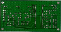
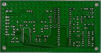
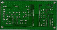
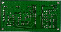
Manufacturing Quality Control: Use the model in electronics manufacturing facilities to inspect PCBs in production lines. The model would recognise and classify defects, assisting in maintaining high standard production quality.
-
Automated Repair Identification: In a Computer Repair Services setup, the model could quickly identify any PCB defects, speeding up the repair process by pinpointing the issues, reducing labor and time.
-
Electronics Education: Use the model as a teaching aid in electronics engineering or similar courses. It would help students understand different common PCB defects, how to identify them, and potentially how they can be fixed.
-
Salvaging E-Waste: The model could be applied in e-waste recycling, to identify defective PCBs that can not be reused. This will help in efficient sorting and collection of electronics waste.
-
Research and Development: In R&D processes, the model could assist in identifying and analyzing defects in prototype electronics, which could accelerate product development and improve reliability of final designs.
Cite This Project
If you use this dataset in a research paper, please cite it using the following BibTeX:
                        @misc{
                            pcb-defect-y2wuo_dataset,
                            title = { PCB Defect Dataset },
                            type = { Open Source Dataset },
                            author = { yolox },
                            howpublished = { \url{ https://universe.roboflow.com/yolox-qcftu/pcb-defect-y2wuo } },
                            url = { https://universe.roboflow.com/yolox-qcftu/pcb-defect-y2wuo },
                            journal = { Roboflow Universe },
                            publisher = { Roboflow },
                            year = { 2023 },
                            month = { jun },
                            note = { visited on 2025-03-07 },
                            }


